Measuring Surface Flatness Using The Fuji Prescale Pressure Measurement System
Keywords: pressure measurement system, surface flatness, pressure mapping Summary: High-volume manufacturing of microelectric and microfluidic devices requires precise dimensions and surface flatness of molds. Using the Fuji Prescale film, engineers can quickly and easily evaluate polymer-manufactured molds for any geometry and surface flatness defects. Source: Sung-Won Youn et. al. A replication process of metallic micro-mold by using parylene embossing and electroplating, Microelectronic Engineering 85 (2008) 161-167.
Written by Igor Mateski
Surface Flatness In Hot Embossing Manufacturing Processes
Manufacturing microelectric and microfiludic devices is a process that has low tolerance to surface imperfections and dimension distortions caused by the materials and processes used. One of the most used microelectric manufacturing process is hot embossing. Because of its technical limitations, engineers study current and related manufacturing processes to further improve hot embossing as a viable and economical large-scale manufacturing process. Below is just a short list of related manufacturing processes that we have done studies of in previous articles:
- micro-fluidic systems (see pressure mapping in micro fluidic manufacturing case study)
- step and stamp (see pressure sealing in medical industry case study)
- rolling (see paper rolling pressure mapping case study)
As with related processes, hot embossing requires high surface flatness. Otherwise, devices will not be manufactured according to specifications. Mold defects can easily occur as result to large surface area of the mold, complex geometry of the product, dust particles, embossing/demolding conditions and so on. These are some of the reasons why engineers are looking for ways to cut costs in manufacturing the molds and avoid surface flatness defects of the final products.
Pressure Mapping In Paralyne-C Master Microstructure Manufacturing
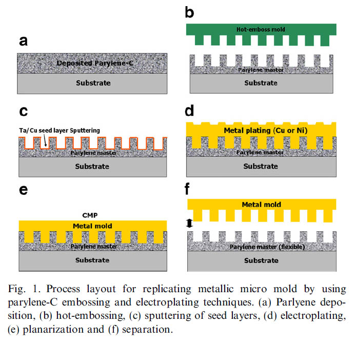
To cut manufacturing costs, some engineering teams have suggested using a polymer based master that can be used for producing metallic molds. These low-cost metallic molds can then be used in manufacturing of micro fluidic and micro electrical devices that have lower chance of surface flatness defects. Below is a diagram of how polycarbonate (PC) masters can be used in producing low-cost metallic molds. The paralyne-C material was used as it has proven to be a great material with high ability to preserve geometric shapes and has solid anti-adhesive properties when in contact with metals.

As the image above shows, a hot-emboss mold is used to imprint the needed structure onto a Parylene-C master. This master has good material properties so when metal molds get produced, they have very good surface flatness and preserve the needed geometry of the structure. Also, thanks to anti-adhesive properties of paralyne-C, the separation of molds goes almost flawlessly.
But as with any other manufacturing process this too needs quality control, so verifying metal mold surface flatness is a good way to ensure production quality. As the reason for polycarbonate based masters in microelectric and microfluidic elements was to cut costs, the process of quality control should also be affordable and fast. This means that testing each master regularly under an electron microscope to evaluate geometry distortions is not feasible.
Using The Fuji Prescale Pressure Measurement System To Evaluate Surface Flatness
A research team from the Advanced Manufacturing Research Institute, part of the National Institute of Advanced Industrial Science and Technology in Japan suggests using the Fuji Prescale Film to evaluate surface flatness of the mold and samples. Using the Fuji Prescale to read surface flatness means that engineers use tactile pressure as a direct indicator of surface flatness.
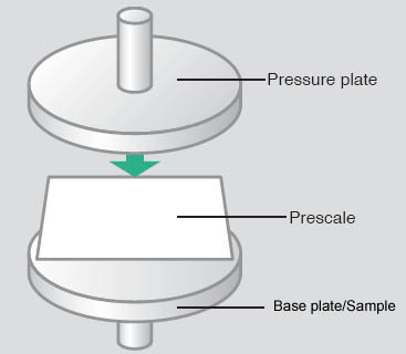
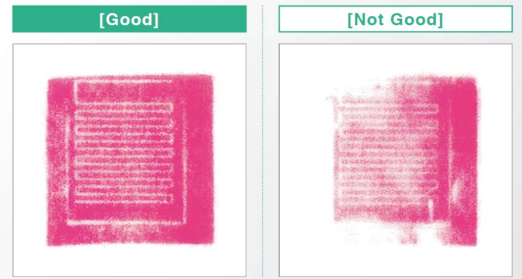
To measure surface flatness using pressure distribution, engineers take a sample part, place over it a Fuji Prescale film cut to shape, and apply pressure to expose the Fuji Prescale film. Once the film is developed, engineers can visually inspect the pressure distribution and evaluate surface flatness.
Below is an illustration of the testing rig used for measuring surface flatness using pressure mapping:

To better understand the pressure profile, engineers can also use the Digital Pressure Distribution Mapping System to measure pressure in specific points of the manufactured sample. This helps engineers check critical points in the part geometry and evaluate if and when the mold has become defective. To use the digital pressure mapping system engineers scan the developed Fuji Prescale film, select the pressure range of the scanned film, and the software works out the exact pressure values based on the redness level and the pressure range of the used film.

Using the developed Fuji Prescale film, engineers can easily evaluate if and when the mold needs replacement. This direct surface flatness measurement helps manufacturing facilities bring the production costs down while keeping high manufacturing quality.
Related Articles:
Digital Pressure Distribution Mapping SystemPressure Mapping in Micro Fluidic Manufacturing
