Using Fuji Prescale in PCB and Electronics Manufacturing
Keywords: : stencil PCB pressure distribution, multi-layer PCB manufacturing, tactile pressure measurementSummary: PCB manufacturing relies on precise tactile pressure for making plastic carbon-leads PCBs as well as standard multi-layered PCBs. With Fuji Prescale, manufacturers finally have a reliable and fast way to determine the pressure distribution and ensure high-quality PCB manufacturing.
Written by Igor Mateski
Tactile Pressure in Electronics Manufacturing
Mixing electronics and tactile pressure sounds unusual, but in reality, high-yield electronics manufacturing is totally dependent on nominal tactile pressure to ensure proper manufacturing processes such as:
- Manufacturing of printed circuit boards
- Combining many layers into a single complex multi-layered PCB
- Mass-positioning of Surface-Mount Devices (SMDs) for small scale electronics
- Sealing of SMD electro-magnetic components in EM shields etc.
Nominal Stencil Pressure and Possible Defects
Nominal stencil pressure in PCB manufacturing can cause various problems such as:
- broken conducting lines
- weakened conductivity in on-board anti-eddy (Foucault) currents wiring
- distorted values of printed inductor coils
For high-precision electronics devices such as smartphones, PCB manufacturers must ensure a manufacturing process that gets the PCB done correctly every time. If the process is not optimized there will be bad end products that can cause major financial and market losses because of all the warranty claims.
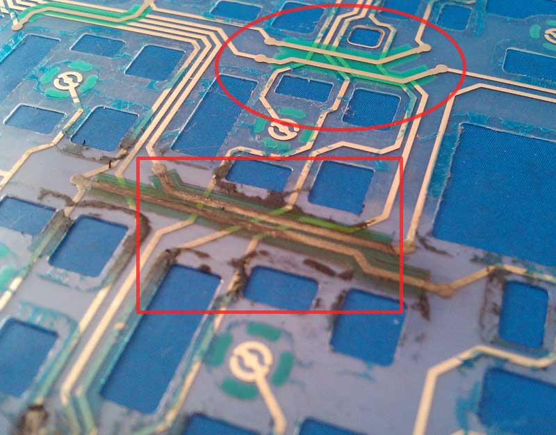
Here is a good example of a defective product that broke a year after purchase. This is a printed circuit board from a PC keyboard, where the wiring is carbon leads printed onto a plastic foil no thicker than a paper sheet.

The image above has two areas of attention.
The area encircled with the red ellipse is an example of a good two-layer wiring where the carbon-based conductors are properly stamped (or printed) onto the plastic substrate. The green base is an insulator over which two conductors are applied to create bridging. The clear conductor contours show a solid printing.
The area in the red rectangle shows another bridging where the second layer of wiring is not properly stamped onto the plastic substrate which caused a break in the circuit. As this is not an isolated case, the laptop manufacturer had enormous losses with all the warranty claims, and had an indelible damage to their brand name which causes even more in lost revenue.
Fuji Prescale Film as Maintenence and QA Tool
As it is not easy to rely on X-ray scans to eliminate all defective PCBs, a better option to ensure high quality is to work proactively in ensuring that the manufacturing process itself is as close to flawless as possible.
The best way to ensure high production quality is to constantly monitor the wiring application onto the substrate, whether that is a photo-lithographic PCB manufacturing or stenciled carbon leads on plastic foils as is the case in laptop keyboards.
In regular PCB manufacturing, service technicians can use Fuji Prescale films to run regular testing of manufacturing processes such as:
- testing the pressure distribution in a PCB lamination press
- test the squeegee pressure distribution in solder cream application machines
- test tactile pressure in the SMD application process
In plastic-substrate PCB manufacturing, Fuji Prescale films can be used to directly measure the pressure of the stencil during the carbon leads adhesion onto the plastic substrate
In both cases of PCB manufacturing, technicians can greatly inmprove the overal output quality and performance. Thanks to smart and regular use of Fuji Prescale flims, PCB manufacturers can reap the benefits:
- Increased productivity thanks to minimal service time
- Improved overall quality of PCBs
- Decreased waste of material thanks to timely and easy defect detection
