Fine Tuning Chemical Mechanical Polishing Head With Fuji Prescale Film
Keywords: wafer polishing, semiconductor production, CMP head repair Summary: Production of semiconductor components relies on evenly polished wafer surface. The wafer polishing process can sometimes result in uneven polishing or even scratching the wafer surface. Using Fuji Prescale films, the CMP head can be properly aligned to improve the production quality. Written by Igor MateskiCMP Head as Quality Assurance in Semiconductor Production
Semiconductor components require clean rooms and high precision machines in order to reach the level of product reliability that will justify high volume manufacturing. In order to reach the product reliability, semiconductor manufacturers use chemical and mechanical polishing process that ensures a clean and perfectly flat wafer surface. Any surface deviance will result in faulty end product, which with high-volume manufacturing can mean losses of entire batches of components.
Because of this high demand on clarity and smoothness of the wafer surface, the CMP head must be perfectly flat and properly aligned with the abrasive pad.
Usually, production technicians would test the production result and evaluate the polishing process based on the examined wafers. This resulted in poor production quality and the defects were diagnosed too late which in turn meant measurable dollar losses due to faulty products.
Using Fuji Prescale to Detect CMP Head Reliability
The standard method of checking for contact uniformity between the wafer and abrasive pad is slow and infective.
In order to improve the quality of production and shorten the time of servicing CMP heads, repair and manufacturing technicians should use the Fuji Prescale film as shown on the image below.
To check the alignment and pressure distribution along the wafer-abrasive pad surface, technicians can use the Fuji Prescale 4LW Film (extremely low pressure sensitivity).
The illustration above shows how to make this measuring: Place the Fuji Prescale 4LW film between the wafer and abrasive pad. Then release the contacting pressure without rotating the Rotating Platen or the Polishing Head Mechanism. This will develop the prescale film, and a quick visual inspection can reveal the state of the wafer-abrasive pad contact profile.
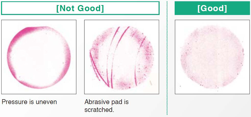
The image below shows two defect scenarios
The image on the left shows a defect with uneven pressure distribution which is caused by an uneven surface of the polishing head. In this case, the head surface itself needs polishing so it gets the perfect flatness needed for high quality polishing of the wafer plates
The middle image reveals a defect on the abrasive pad surface. The scratches are in fact ridges where the pressure is highest, and therefore the abrasive power is strongest along these lines. This will result in defective wafer surface. To repair this problem the abrasive pad needs to be replaced.
Finally, the image on the right displays the proper pressure profile and only in this case the polished wafers can be used to produce reliable semiconductor components
Benefits of Using Fuji Prescale in Semiconductor Production
From the images above, it is obvious that using the Fuji Prescale film in semiconductor manufacturing has numerous benefits:
- Thanks to the Fuji Prescale, the manufacturing process is more reliable
- With Fuji Prescale films, defective polishing machines can be easily diagnosed
- The Fuji Prescale flim greatly shortens the repair process so manufacturing can resume as soon as possible
Using Fuji Prescale 4LW films in semiconductor manufacturing will ensure high quality of the semiconductor components, high manufacturing rate, and minimal losses due to equipment servicing.

