Avoiding Manufacturing Defects of Multi-layer PCB With Fuji Prescale
Keywords: : stacking machine, pcb manufacturing defects, stacking machine head testingSummary: PCB manufacturing machines ware and tare result in poor quality and material loss. Using Fuji Prescale films manufacturers can ensure proper lamination thanks to nominal pressure profile checking without costly retrospective diagnosis processes.
Written by Igor Mateski
Multi-Layered Electronic Components Manufacturing
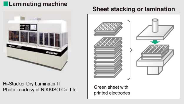
Multi-layering (lamination) is a process that is widely used in manufacturing various electronic components:
- Ceramic capacitors
- LCD screens
- Multi-layered PCBs
- Touch-sensitive pads
In all of these products, the precision and reliability of electronic components and assemblies depends on the precision of manufacturing.
In some cases, like in capacitor manufacturing, lamination press pressure distribution is of utmost importance so that the stacked layers adhere properly otherwise the nominal capacity of each produced capacitor may vary outside the prescribed nominal tolerance.
Defects in Multi-Layered PCBs
Similar to ceramic capacitor manufacturing, multi-layered PCBs are also sensitive to pressure balance deviations. This sensitivity grows as the number of stacked layers increase.
PCB layers stacking is a process of joining electrical wiring in 3D where horizontal alignment of contact pads is extremely important so that all layers are properly bridged for proper operation of the final multilayered PCB.

As with any other manufacturing process, PCB stacking machines are subject to ware and tare which results in poor pressure balance. Depending on the size of the PCB, this pressure balance deviation can result in sporadic defective PCBs or total breakdown of the manufacturing process if/when the pressure disbalance is so great that every PCB is defective.
The scale of PCB contact pads (electrodes) is so small that visual inspection cannot determine if the stacking machine is off-balance and the only way to test for manufacturing errors is to run full diagnostics on the manufactured batch and establish a precise diagnostics of where the tactile pressure is off-balance.
The problem is that such a diagnostic is retrospective, and relies on already manufactured PCBs as diagnostic tool to evaluate if the stacking machine exerts nominal pressure on the entire PCB surface. Such diagnostics is both expensive and time consuming, during which the manufacturing process has to stop in order to prevent further loss of material.
Fuji Prescale Film As Diagnostics Tool in PCB Manufacturing
To avoid material losses with the expensive retrospective diagnostics of stacking machines, maintenance technicians should use a direct pressure distribution measurement.
Direct tactile pressure measurement will eliminate the need of testing batches of defective PCBs to get to a proper diagnosis, and the only reliable way to do direct pressure measurement is to use the Fuji Prescale pressure sensitive films. There are several pressure ranges to choose from, depending on the nominal pressure the lamination press exerts on the PCB layers. Usually, PCB manufacturers use one of the three pressure sensitive films (to see pressure ranges please visit the Prescale Pressure Ranges page
- Fuji Prescale Super Low Pressure (LLW)
- Fuji Prescale Low Pressure (LW)
- Fuji Prescale Medium Pressure (MW and MS)
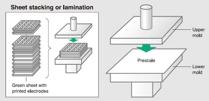
Below is an illustration of how the Fuji Prescale film should be used:

The Fuji prescale film is cut to size and placed between the stacking machine upper and lower working surfaces. The nominal pressure is applied and the developed Fuji Prescale film is ready for visual inspection or for scanning in the Fuji FPD-8010E Digital Pressure Mapping System for precise pressure values or 3D visualization of the pressure profile.
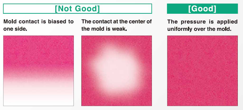
Below is an image of developed Fuji Prescale films of a stacking machine that underwent maintenance:

Stacking machines can have two basic defects: biased pressure and bulging/denting of the stacking surface.
The image on the far left is from a stacking machine that exerts more pressure at one end, while the other end of the tactile surface is left with pressure below the nominal tactile pressure. In this case PCB stacks can experience two types of defects:
- cracking due to higher than nominal pressure, or
- poor adhesion of electrodes due to lower than nominal pressure
In the mid photo, the stacking head is dented inward so the central area of the head does not exert the nominal pressure onto the PCB stack. In this case the contact pads in the central area will not be adhered properly and the PCB will not conduct electricity properly. When this defect occurs the stacking head needs replacement.
The image on the right is from a properly working stacking machine where it is visible that the entire surface exerts the nominal pressure and manufactured PCBs will be of high quality.
Thanks to Fuji Prescale pressure sensitive films, maintenance technicians can quickly and regularly run tests to ensure proper operation of the stacking machine so each and every PCB meets the manufacturing criteria.
